Growth of nanowires
1. The vapour–liquid–solid growth method Semiconductor
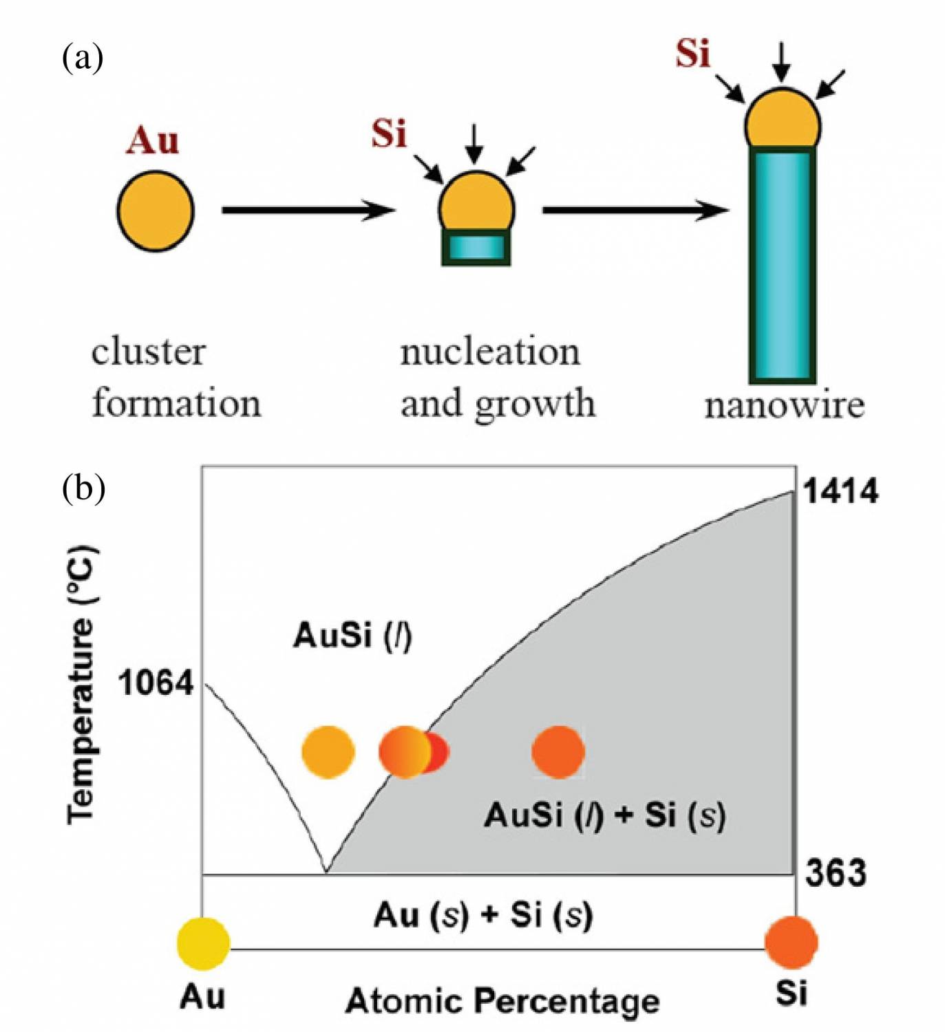
Semiconductor NWs are generally synthesized by employing metal nanoclusters as catalysts via a vapour–liquid–solid (VLS) process (figure 1) [6]. In this process, the metal nanoclusters are heated above the eutectic temperature for the metal–semiconductor system of choice in the presence of a vapour-phase source of the semiconductor, resulting in a liquid droplet of the metal/semiconductor alloy. The continued feeding of the semiconductor reactant into the liquid droplet supersaturates the eutectic, leading to nucleation of the solid semiconductor. The solid–liquid interface forms the growth interface, which acts as a sink causing the continued semiconductor incorporation into the lattice and, thereby, the growth of the nanowire with the alloy droplet riding on the top.
 The gaseous semiconductor reactants can be generated through decomposition of precursors in a chemical vapour deposition (CVD) process or through momentum and energy transfer methods such as pulsed laser ablation [7] or molecular beam epitaxy (MBE) [8] from solid targets. So far, CVD has been the most popular technique. In CVD–VLS growth, the metal nanocluster serves as a catalyst at which site the gaseous precursor decompose, providing the gaseous semiconductor reactants. In the case of SiNW growth (figure 1), silane (SiH4) and Au nanoparticles are normally used as the precursor and catalysts, respectively. Besides group IV materials, compound III–V and II–VI NWs have also been produced with the VLS method, in which pseudobinary phase diagrams for the catalyst and compound semiconductor of interest are employed. In the compound semiconductor case, metal-organic chemical vapour deposition (MOCVD) [9] or pulsed laser ablation [10] are typically used to provide the reactants.
 There are two competing interfaces during nanowire growth, the liquid/solid interface between the eutectic and the nanowire and the gas/solid interface between the reactants and the exposed surface of the growing nanowire. Precipitation through the first interface results in the VLS growth and axial elongation of the nanowire, while dissociative adsorption on the second interface results in vapour–solid growth and thickening in the radial direction. Either mechanism can be dominating in an actual growth process, depending on the detailed growth condition such as the pressure, flow rate, temperature, reactant species and background gases that are by-products of growth reactions. For example, in the above- mentioned SiNW growth process, low temperature growth can reduce the rate of direct thermal dissociation of silane; hence, axial nanowire growth is favoured. Hydrogen has also been found to mitigate radial growth through suppression of either the adsorption of the reactants by terminating the Si surface [11] or of the dissociation of silane [12,13]. The use of H2 as the carrier gas also passivates theNWsurface in a manner similar to that observed in thin-film growth [14] and reduces roughening along the NW. Uniform NWs with negligible diameter variation can thus be achieved through careful control of the growth conditions, including the employment of local heaters to reduce uncontrolled decomposition of silane [15]. On the other hand, tapered NWs are products from simultaneous growth in both the axial and radial directions and are generally not desirable for most electrical and optical applications. In the CVD–VLS growth process the diameter of the
nanowire is determined by that of the starting nanocluster, and uniform, atomic-scale NWs can be obtained in a well- controlled growthprocess as nanoclusters with diametersdown to a fewnanometres are nowcommercially available. Wu et al reported growth of uniform SiNWs with diameters down to 3nm[11] using SiH4 as the precursor and H2 as the carrier gas. Wu performed detailed high-resolution transmission electron micrography (HRTEM) studies on these SiNWs and observed that the NWs are single-crystalline with little or no visible amorphous oxide even at this scale. The resulting SiNWs
shownarrowsize distributions of 13.2±1.7 nm, 5.9±1.1 nm, and 4.6 ± 1.2 nm, respectively when gold nanoclusters of diameters of 10 (9.7 ± 1.5) nm, 5 (4.9 ± 0.7) nm, and 2 (3.3 ± 1)nm are used. The increase in the NW diameters compared with those of the starting nanoclusterswas attributed
to the supersaturation of silicon in gold nanoclusters during the formation of the liquid droplet prior to nucleation, an effect observed previously with in situ observations of the growth of germanium NWs [16]. The crystallographic orientation of the NW during VLS
growth is chosen to minimize the total free energy, as the process is thermodynamically driven. The total free energy includes the ‘bulk’ energy of the SiNW, the Au/Si interface energy and the Si/vacuum interface energy. In Wu’s study, the growth directions of SiNWs with different diameters are carefully examined [11]. Ahistogram of the growth directions of the SiNWs is shown in figure 2. Prior studies of VLS growth on micrometre-scale silicon whiskers have shown that
the growth is primarily along the ?111? direction, since the solid–liquid interface parallel to a (111) plane possesses lowest free-energy [6]. The predominant ?111? growth direction (figure 2(e)) and the single (111) plane at the catalyst/NW
interface (figure 3(a)) were indeed observed on VLS-grown SiNWs as well, with diameters larger than 20nm [11]. On the
other hand, ?110? becomes the predominant growth direction for NWs with diameter smaller than 10nm (figure 2(c)). This phenomenon can be explained by the fact that the Si/vacuum surface energy becomes increasingly dominating when the surface/volume ratio is increased as the nanowire diameter
is decreased, as the Si/vacuum surfaces parallel to ?111? axis consist of the lowest free-energy (111) and (100) planes
(figures 3(c) and (d)). Interestingly, ?110? growth does not arise from the formation of a liquid/solid (110) interface. As shown in figure 3(b), the catalyst/NW interface now consists of two low energy {111} planes, whereby the ?111? and
?11 − 1? directions combine to yield a growth axis of ?110?. Such observations are consistent with the thermodynamic
picture of the VLS growth mechanism. The ?112? growth direction, which is observed for a substantial fraction of intermediate-diameter SiNWs (figure 2(d)), can be explained
as a ‘transitional’ direction between the ?111? and ?110? growth directions since the (112) plane is a stepped plane between the (111) and (110) planes [17].
2. Nanowire heterostructures
Compared with nanostructures fabricated from other ap- proaches such as vapour–solid growth [18] or solution based liquid–solid growth [19], the VLS process offers one key advantage—heterostructures can be achieved at the individual device level ina controlled fashion. Both axial heterostructures (figures 4(c) and (e)), in which sections of different materials with the same diameter are grown along the wire axis [20,21], and radial heterostructures (figures 4(d) and (f )), in which core/shell and core/multi-shell form along the radial direction [22–24], have been realized on VLS–CVD grown NWs. To understand the rational formation of nanowire heterostructures within the context of the VLS method, consider the possible effects of a change in reactant vapour once nanowire growth has been established (figure 4). If vapour decomposition/adsorption continues exclusively at the surface of the catalyst nanocluster site, crystalline growth of the new semiconductor will continue along the axial direction (figure 4(c)). On the other hand, if the decomposition of the new vapour/reactant on the surface of the semiconductor nanowire cannot be neglected, a shell of material will grow on the original nanowire surface (figure 4(d)). Repeated changing of reactants in a regime favouring axial growth will lead to the formation of a nanowire superlattice, as shown in figure 4(e), while changing reactants in a radial-growth regime will result in core-multi-shell radial structures, as shown in figure 4(f). It is important to mention that there are few constraints on the composition of the shell growth; any material suitable for planar film deposition can be deposited on the surface of a nanowire, and crystalline radial heteroepitaxy [22] can be achieved as the nanowire surface is crystalline.
2.1. Radial nanowire heterostructures.
Radial core/shell heterostructures can be achieved if dissociation of the reactants is promoted at the grown nanowire surface (figure 4(d)) [22], analogous to the layered growth of planar heterostructures. Compared with NWs in the simple homogeneous form, core/shell heterostructure NWs offer better electrical and optical properties as they can now be tailored through band structure engineering. For example, similar to the formation of two-dimensional electron [26] and hole gases [27] in high- electron mobility transistors (HEMTs), 1D electron and hole gases can be achieved in core/shell heterostructure NWs. Lu et al observed that a 1Dhole gas [23] will be formed if aSi shell is epitaxially grown on top of a Ge core, as shown in figure 5. Thevalence band offset of ca500meVbetweenGeand Si at the heterostructure interface [27,28] then serves as a confinement potential for the quantum well, and free holes will accumulate in the Ge channel when the Fermi level lies below the valance band edge of the Ge core (figure 5(B)). In the Ge/Si core/shell nanowire heterostructure, the pseudomorphic strain in the epitaxial core and shell materials is relaxed along the radial direction [22], yielding a type II staggeredbandalignment [27]. The light hole and heavy hole bands are expected to split due to the effects of strain and confinement [27]. This hole-gas system will be discussed in detail in section 3.2, as novel phenomena and high-performance transistors are realized on such core/shell NWs. Other types of core/shell nanoires have also been studied.
For example, GaN based core/multi-shell NWs [24, 29]have been grown using MOCVD. High-efficiency light-emitting diodes were obtained on these core/multi-shell structures using bandstructure engineering and modulation doping [24, 29]. In a different approach, silicon/silica core/shell NWs were produced through thermal oxidation of as-grown SiNWs [30, 31]. By treating either the silica shell or the silicon core as a sacrificial material, silica nanotubes [31] or parallel array of silicon NWs with controlled spacing [30] have been demonstrated, respectively.
For example, GaN based core/multi-shell NWs [24, 29]have been grown using MOCVD. High-efficiency light-emitting diodes were obtained on these core/multi-shell structures using bandstructure engineering and modulation doping [24, 29]. In a different approach, silicon/silica core/shell NWs were produced through thermal oxidation of as-grown SiNWs [30, 31]. By treating either the silica shell or the silicon core as a sacrificial material, silica nanotubes [31] or parallel array of silicon NWs with controlled spacing [30] have been demonstrated, respectively.
2.2. Axial nanowire heterostructures. Unlike radial het- erostructures in which the shell growth does not involve reac- tion with the nanocluster catalyst, axial nanowire heterostruc- tures can be obtained by alternative introduction of vapour phase reactants that react with the same nanocluster catalyst, as illustrated in figures 4(c) and (e). A critical requirement of the axial nanowire heterostructure growth is then that a single nanocluster catalyst can be found which is suitable for growth of the different components under similar conditions. For a wide range of III–V and IV materials, Duan et al observed [10] that Au nanoclusters can meet this requirement. Using Au nanoclusters as catalysts and a laser-assisted catalytic growth, Gudiksen et al [20]have successfully obtained GaAs/GaP axial nanowire heterostructures (superlattices) with GaAs and GaP targets at temperatures of 700–850 ◦C at 100Torr in a contin- uous argon flow. Figure 6(a) shows a TEM image of a typical GaAs/GaP junction region obtained by Gudiksen. The nanowire axes
was found to lie along the ?111? direction, in agreement with previous studies of single-component systems [7,10,32]. Two-dimensional Fourier transforms calculated from high- resolution images containing the junction region (figure 6(a), inset) showpairs of reciprocal lattice peaks along the different lattice directions, while such transforms calculated from the regions above and belowthe junction (not shown) exhibit only single reciprocal lattice peaks. Analysis of these peak data yields lattice constants, indexed to the zinc blende structures
of GaP and GaAs, of 0.5474 ± 60.0073nm and 0.56686 ± 0.0085nm and are in good agreement with the values for both GaP (0.5451 nm) and GaAs (0.5653 nm), respectively. Local elemental mapping of the heterojunction by energy
dispersive x-ray spectroscopy (EDS) was carried out to probe composition variations across the heterostructure junction (figures 6(b)–(e)). The elemental maps show that Ga is uniformly distributed along the length of the NW, while P (figure 6(d)) and As (figure 6(e)) appear localized in the GaP and GaAs portions of the nanowire heterostructure, respectively. Quantitative analysis of thePandAscomposition
variation (figure 6(f)) however, shows, that the junction is not atomically abrupt but rather makes the transition between GaP and GaAs phases over a length scale of 15–20 nm. This length scale is consistent with the hypothesis
that the ∼20nm diameter Au catalyst must re-alloy with GaP after initial GaAs growth. The observed composition variation has several potentially important implications. First, composition variation at the interface can relieve strain and may enable the defect-free junctions and superlattices that were observed in the GaAs/GaP system which has a relatively large lattice mismatch. Second, the observed composition variation could be substantially reduced in smaller-diameter NWs when abrupt interfaces are required in certain photonic and electronic applications. For example, a 5nm diameter nanowire superlattice should have variations of 5 nm across the junction interfaces. Alternatively, it should be possible to use different nanocluster catalysts or variations in the growth temperature when reactants are switched to obtain sharper interfaces. By repeating the modulation process, nanowire superlat-
tices canbeproduced inwhichthenumberof periodsandrepeat spacing can be readily varied during growth. For example, Gudiksen et al demonstrated a 21-layer GaAs/GaP superlat- tice with arbitrary repeat spacing, with the lengths of the seg- ments controlled by the number of pulses delivered to each target. In an independent study, the Yang group at UC Berke- ley combined thermal CVD using silicon tetrachloride (SiCl4) with the laser ablation of a solid germanium target to pro- duce Si–SiGe NWs [33]. Wire growth was at 850–950 ◦C and 1 atm total pressure, with a SiCl4/H2 mole ratio of 0.02. InP– InAs superlattices with very abrupt interfaces were produced by the Samuelson group at Lund University using ultra-high vacuum chemical beam epitaxy [34]. Wire growth catalysed by Au particles was performed at 420 ◦C and ca 3Torr using trimethylindium (TMIn), tertiarybutylphosphine and tertiary- butylarsine precursors. To create heterojunctions, the TMIn source was turned off, the group V source turned on after a 5 s pause and the TMIn turned on again after another 5 s. HRTEM images were consistent with interface widths of a few atomic layers, though elemental analysis was not performed. The monolayer sharpness of the interfaces was attributed to the high vapour pressures of the group V source materials in combination with the low growth rate (ca 1MLs−1). Such nanowire superlattices offer potential as novel thermoelectric devices [35], resonant tunnelling diode (RTD) devices [36], QDdevices [37,38] or simply as optical nanobarcodes in which information is coded in the length and spacing of the direct bandgap GaAs segments.Besides semiconductor heterostructures, metal/semi-
conductor axial heterostructures and superlattices have also been demonstrated recently [39]. Wuet al observed that NiSi, a bulk metal, can be transformed from Si via solid phase reaction with Ni. As a result, metallic NiSiNWswere produced by first evaporating Ni on SiNWs, followed by heating the sample above the NiSi transisiton temperature [39]. A temperature of 550 ◦C was used in Wu’s study. HRTEM studies verified the resulting wires are single-crystalline NiSi, and transport measurements verified the resistivity is consistent with the bulk NiSi value. Using the same approach, Wu obtained NiSi/Si metal/semiconductor axial heterostructures by selectively patterning Ni on SiNWs using a pre-defined mask, followed by the solid phase reaction process to create NiSi segments at the selected locations. In this case, the interface at the Si/NiSi heterostructure is not limited by diffusion through the catalyst nanocluster and can be atomic sharp [39]. Compared with devices using external microscale leads and interconnects, the NiSi/Si metal/semiconductor heterostructure offers an intriguing solution in which the metallic regions can be used as local contacts to the active semiconductor regions as well as interconnects, hence achieving much higher device density.
2.3. Branched nanowire structures. Branched and tree- like nanowire structures may be obtained if after the initial nanowire growth, metal catalyst nanoclusters are deposited again on the surfaces of the grown NWs (the trunks), and reactants are introduced once more to facilitate nucleation and directional growth of nanowire branches. Epitaxial growth of the branches can occur if the trunk and branches are composed of similar materials and no amorphous overcoating (e.g. oxides) is developed before the branch growth. Branched NWs and ‘nanotrees’ were independently studied by Wang et al in the case of Si and GaN and Dick et al in the case of GaP [40] using MOCVD and a sol–gel method to deposit Au catalyst nanoclusters on the nanowire trunks.
3. Growth of metal oxide NWs
Besides the VLS approach, a simple thermal evapora- tion/vapour transport deposition approach has also been shown to be effective in growing 1D structures, in particular metal oxide (e.g. ZnO, In2O3 and SnO2) NWs. Such NWs have been studied in applications ranging from optoelectronics devices [41–44], field-effect transistors [45,46], ultra-sensitive nanoscale gas sensors [45, 47–50] and field emitters [51, 52]. In particular,ZnONWshave attracted a lot of interest due to the large exciton binding energy (60 meV), high electromechani- cal coupling constant and resistivity to harsh environment [53]. The first attempt to produce ZnO NWs was based on
an electrochemical method using anodic alumina membranes (AAM) [54]. Later on, high-density, ordered ZnO nanowire arrays were obtained using AAM in a vapour-deposition process [55]. However, the AAM approach is typically limited to generating polycrystalline NWs. To produce single- crystalline 1D ZnO nanostructures, a number of methods have been explored such as thermal evaporation/vapour transport deposition [18, 56], hydrothermal process [57], MOCVD [58,59], pulsed laser deposition [60] and MBE [61]. Among all methods used to grow metal oxide NWs,
thermal evaporation/vapour transport deposition has gained the most popularity. The thermal evaporation technique is based on a simple process in which source materials in the condensed or powder form are first vapourized at an elevated temperature; the resulting materials in vapour phase then condense under the right conditions (temperature, pressure, atmosphere, substrate, etc) to form the desired product [62]. The processes are usually carried out in a setup as shown in figure 7, which includes a horizontal tube furnace, a quartz or alumina tube, gas supplies and control system. Single-crystalline ZnO NWs grown with the thermal
evaporation method (referred also as the physical vapour deposition method) were first reported in 2001 [18], with an average diameter of about 60 nm. In 2002, Yao et al reported mass production of ZnO NWs, nanoribbons and needle-like nanorods by thermal evaporation of ZnO powders mixed with graphite [63]. Yao found that temperature was the critical experimental parameter for the formation of different morphologies of ZnO nanostructures. Banerjee et al succeeded in producing grams of ZnO NWs via thermal evaporation of ZnO powder in a tube furnace at high temperatures [64]. Thegraphite flakes were found to be the key ingredient for large-quantity growth and can be easily removed by oxidation at ∼700 ◦C for 1–3 h in O2 flow. Recently, Wan et al reported that single crystalline ZnO
NWs in the kilogram range can be obtained through direct thermal evaporation of metal zinc pellets (purity: 99.999%) at 900 ◦C in a quartz tube [65]. Such an approach provides an effective method for large-scale industrialization without the need of metal catalysts, graphite additives or vacuum. Oxygen ambient was found to be critical for the morphology of the synthesized ZnO products. For example, tetrapod-like ZnO nanostructures were the only product that can be grown in air ambient. However, if Zn pellets were evaporated in 1–5% oxygen, massive wire-like ZnO nanostructures can be obtained.
[6] Wagner R S 1970 Whisker Technology (New York:Wiley)
[7] Morales AMand Lieber CM1998 Science 279 208
[8] Liu J L, Cai S J, Jin G L, Thomas S G andWang K L 1999 J. Cryst. Growth 200 106
[9] Haraguchi K, Katsuyama T, Hiruma K and Ogawa K 1992 Appl. Phys. Lett. 60 745
[10] Duan X and Lieber CM2000 Adv. Mater. 12 298
[9] Haraguchi K, Katsuyama T, Hiruma K and Ogawa K 1992 Appl. Phys. Lett. 60 745
[10] Duan X and Lieber CM2000 Adv. Mater. 12 298
[11] Wu Y, Cui Y, Huynh L, Barrelet C J, Bell D C and Lieber CM 2004 Nano Lett. 4 433
[12] Wang DW,Wang Q, Javey A, Tu R, Dai H, Kim H, McIntyre P C, Krishnamohan T and Saraswat K C 2003 Appl. Phys. Lett. 83 2432
[13] Greytak A B, Lauhon L J, GudiksenMS and Lieber CM2004 Appl. Phys. Lett. 84 4176
[14] Yamanaka M, Sakata I and Sekigawa T 2000 Japan J. Appl. Phys. 39 3302
[15] Yang C, Zhong Z and Lieber CM2005 Science 310 1304
[16] Wu Y and Yang P 2001 J. Am. Chem. Soc. 123 3165
[17] Tan T Y, Lee S T and Gosele U 2002 Appl. Phys. A 74 423
[18] Kong Y C, Yu D P, Zhang B, FangWand Feng S 2001 Appl. Phys. Lett. 78 407
[19] Qian C, Kim F, Ma L, Tsui F, Yang P and Liu J 2004 J. Am. Chem. Soc. 126 1195
[20] GudiksenMS, Lauhon L J,Wang J, SmithDCand Lieber CM2002 Nature 415 617
[21] Wu Y, Fan R and Yang P 2002 Nano Lett. 2 83
[19] Qian C, Kim F, Ma L, Tsui F, Yang P and Liu J 2004 J. Am. Chem. Soc. 126 1195
[20] GudiksenMS, Lauhon L J,Wang J, SmithDCand Lieber CM2002 Nature 415 617
[21] Wu Y, Fan R and Yang P 2002 Nano Lett. 2 83
[22] Lauhon L J, GudiksenMS,Wang C L and Lieber CM2002 Nature 420 57
[23] LuW, Xiang J, Timko B P,Wu Y and Lieber CM2005 Proc. Natl. Acad. Sci. USA 102 10046
[24] Qian F, Gradecak S, Li Y,Wen C Y and Lieber CM2005 Nano Lett. 5 2287
[25] Lauhon L J, GudiksenMS and Lieber CM2004 Phil. Trans. R. Soc. Lond. A 362 1247
[26] Dingle R, Stormer H L, Gossard A C andWiegmannW1978 Appl. Phys. Lett. 33 665
[27] Sch¨ affler F 1997 Semicond. Sci. Technol. 12 1515
[28] Van deWalle C G and Martin RM1986 Phys. Rev. B 34 5621
[29] Qian F, Li Y, Gradecak S,Wang D, BarreletCJand Lieber CM2004 Nano Lett. 4 1975
[30] Whang D, Jin S and Lieber CM2003 Nano Lett. 3 951
[30] Whang D, Jin S and Lieber CM2003 Nano Lett. 3 951
[31] Fan R,Wu Y Y, Li D Y, Yue M, Majumdar A and Yang P 2003 J. Am. Chem. Soc. 125 5254
[32] GudiksenMS and Lieber CM2000 J. Am. Chem. Soc. 122 8801
[32] GudiksenMS and Lieber CM2000 J. Am. Chem. Soc. 122 8801
[33] Wu Y, Fan R and Yang P 2002 Nano Lett. 2 83
[34] BjorkMT, Ohlsson B J, Sass T, Persson A I, Thelander C, MagnussonMH, Deppert K,WallenbergLRand Samuelson L 2002 Nano Lett. 2 87
[35] Li D,Wu Y, Fan R, Yang P and Majumdar A 2003 Appl. Phys. Lett. 83 3186
[36] BjorkMT, Ohlsson B J, Thelander C, Persson A I, Deppert K, Wallenberg L R and Samuelson L 2002 Appl. Phys. Lett. 81 4458
[37] Thelander C, Martensson T, BjorkMT, Ohlsson B J, LarssonMW,Wallenberg L R and Samuelson L 2003 Appl. Phys. Lett. 83 2052
[38] Thelander C, Nilsson H A, Jensen L E and Samuelson L 2005 Nano Lett. 5 635
[39] Wu Y, Xiang J, Yang C, LuWand Lieber CM2004 Nature 430 61
[40] Dick K A, Deppert K, LarssonMW, Martensson T, SeifertW, Wallenberg L R and Samuelson L 2004 Nature Mater. 3 380
[41] Kind H, Yan H Q, Messer B, LawMand Yang P 2002 Adv. Mater 14 158
[42] Keem K, Kim H, Kim G T, Lee J S, Min B, Cho K, SungMY and Kim S 2004 Appl. Phys. Lett. 84 4376
[43] ParkWI and Yi G C 2004 Adv. Mater. 16 87
[44] Konenkamp R,Word R C and Schlegel C 2004 Appl. Phys. Lett. 85 6004
[45] ArnoldMS, Avouris P, Pan ZWandWang Z L 2003 J. Phys. Chem. B 107 659
[46] Park J Y, Yun Y S, Hong Y S, Oh H, KimJJand KimSS 2005 Appl. Phys. Lett. 87 123108
[47] Li Q H, Liang Y X,Wan Q,Wang T H 2004 Appl. Phys. Lett. 85 6389
[48] Wan Q, Li Q H, Chen Y J,Wang T H, He X L, LiJPand Lin C L 2004 Appl. Phys. Lett. 84 3654
[49] Wang H T, Kang B S, Ren F, Tien L C, Sadik PW, Norton D P, Pearton S J and Lin J 2005 Appl. Phys. Lett. 86 243503
[50] Fan Z Y and Lu J G 2005 Appl. Phys. Lett. 86 123510
[51] Lee C J, Lee T J, Lyu S C, Zhang Y, Ruh H and Lee H J 2002 Appl. Phys. Lett. 81 3648
[52] Jo S H, Lao J Y, Ren Z F, Farrer R A, Baldacchini T and Fourkas J T 2003 Appl. Phys. Lett. 83 4821
[53] Ozgur U, Alivov YI, Liu C, Teke A, Reshchikov MA, Dogan S, Avrutin V, Cho S J and Morkoc H 2005 J. Appl. Phys. 98 041301
[54] Li Y, Meng GW, Zhang L D and Phillipp F 2000 Appl. Phys. Lett. 76 2011
[55] Liu C H, Zapien J A, Yao Y, Meng XM, Lee C S, Fan S S, Lifshitz Y and Lee S T 2003 Adv. Mater. 15 838
[56] Pan ZW, Dai S, Rouleau CMand Lowndes D H 2005 Angew. Chem. Int. Edn. Engl. 44 274
[57] Yang M, Pang G S, Jiang L F and Feng S H 2006 Nanotechnology 17 206
[58] ParkWI, Kim D H, Jung SWand Yi G C 2002 Appl. Phys. Lett. 80 4232
[59] Kim SW, Fujita S and Fujita S 2005 Appl. Phys. Lett. 86 153119
[60] Liu ZW, Ong C K, Yu T and Shen Z X 2006 Appl. Phys. Lett. 88 053110
[61] Heo YW, Varadarajan V, Kaufman M, Kim K, Norton D P, Ren F and Fleming P H 2002 Appl. Phys. Lett. 81 3046
[62] Dai Z R, Pan ZWandWang Z L 2003 Adv. Funct. Mater. 13 9
[60] Liu ZW, Ong C K, Yu T and Shen Z X 2006 Appl. Phys. Lett. 88 053110
[61] Heo YW, Varadarajan V, Kaufman M, Kim K, Norton D P, Ren F and Fleming P H 2002 Appl. Phys. Lett. 81 3046
[62] Dai Z R, Pan ZWandWang Z L 2003 Adv. Funct. Mater. 13 9
[63] Yao B D, Chan Y F andWang N 2002 Appl. Phys. Lett. 81 757
[64] Banerjee D, Lao J Y,Wang D Z, Huang J Y, Ren Z F, Steeves D, Kimball B and SennettM2003Appl. Phys. Lett. 83 2061
[65] Wan Q, Lin C L, Yu X B andWang T H 2004 Appl. Phys. Lett. 84 124
[65] Wan Q, Lin C L, Yu X B andWang T H 2004 Appl. Phys. Lett. 84 124