Application of lateral photovoltaic effect to the measurement of the physical quantities of p-n junctions - Sheet Resistivity and junction conductance of N2+ implanted Si
Hirohiko Niu, Tetsuro Matsuda, Hideaki Sadamatsu and Munezo Takai
A new method of measuring the physical quantitites of a thin film p-n junction shuch as the one formed by ion implantation has been developed; by means of this method difficulties of making reliable electrical contacts with thin layers and leakage currents which are often encountered when applying the bias voltage can be avoided.
Lucovsky's theory for the lateral photovoltaic effect has been extended such that nonzero values for sheet resistivities of both p and n layers and a finite value for the length of the junction are taken into consideration, and the modified theory has been experimentally verified using p-Si samples implanted with N2+ at 8 keV. With the aid of the theory, sheet resistivities, junction conductances and some other physical quantities are obtained by analysing the measured lateral photovoltage (LPV). The use of the LPV method together with the ordinary one increases the reliability of the measurement.
1. Introduction
Measurements of electrical properties of a p-n junction such as formed by ion implantation are often accompanied with difficulties of making reliable electrical contacts to the p or n layer especially when one of the layers is extremely thin; the contacts are apt to penetrate the layer in the process of alloying and it is not easy to confirm whether the contacts are ohmic. Furthermore, the bias voltage applied to the junction is liable to cause leakage currents. These undesirable factors can be avoided by a newly proposed method using the following lateral photovoltaic effect.
Измерения электрических свойств p-n-перехода, таких как образующихся при ионной имплантации часто сопровождается трудностями создания надежных электрических контактов к p или n слой, особенно когда один из слоев является чрезвычайно тонкой; контакты, склонны проникать в слой в процессе сплавления, и это не легко подтвердить, является ли контакты омические. Кроме того, напряжение смещения, приложенное к перекрестку может вызвать возникновение токов утечки. Эти нежелательные факторы, можно избежать с помощью предложенного нового способа с использованием следующего бокового фотоэлектрический эффект.
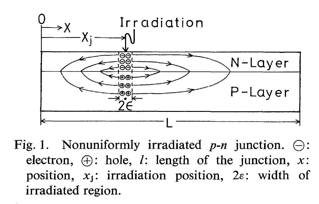
Lateral photovoltaic effect (subsequently represented by LPE) has been found by Wallmark;[1] as well be illustrated with Fig. 1, a nonuniform irradiation on the junction produces a photovoltage parrallel to the junction, i.e. the lateral photovoltage (LPV), in addition to the photovoltage between the p and n layers, i.e. the transversal photovoltage. A theoretical treatment for LPE has been carried out by Lucovsky, [2] (but for a special case). In measuring the LPV, it is clear that the electrical contacts to one of the layers (the implanted layer in the present case) can be ommited and no bias is needed, and the LPV will give informations about junction properties. This is the reason why we have attempted to adopt LPE.
In previous papers, [3,4] we have confirmed by the use of LPE that an n-type layer is formed by nitrogen-ion implantation into silicon. These works, however, have given only qualitative results. In the present paper in contrast to them, quantitative treatments will be given , the outline of which is as follows:
(1) Lucovsky's theory is modified in some respects. His theory is based on the assumptions that the length of the junction is infinite comparing with its width and the one side layer (the implanted layer in our case) is equipotential due to its low resistivity. These assumptions, however, are hardly realized in the p-n junctions; when the one side layer (the implanted layer) is extremely thin the lateral resistance of the layer is not negligible, even if the layer is of low resisitivity. In practice, as will be shown later, we have observed at samples (silicon implanted with N2+ at 8 keV) the implanted layer is not equipotential and the LPV generated in the implanted layer is higher than that in the substrate. (This observation is possible without above mentioned electrical contacts to the implanted layer.) Therefore, in estabilishing a new theory we take nonzero values for the sheet resistivities of both p and n layers and a finite value for the length of the junction.
(2) Experimental verifications of the new theory are made using nitrogen-ion implanted silicon samples.
(3) The measured LPV's are analyzed with the aid of the theory and the conductance of the junction are obtained.
(4) The sheet resistivity and the conductance thus obtained are compared with the values measured by the ordinary methods (van der Pauw's method5) and the method of measuring I-v characteristics of diodes).
2. Theoretical
We will consider a nonuniformly irradiated p-n junction as shown in Fig. 1. The optically generated hole-electron pairs are separated by the built-in potential as they reach the junction by diffusion; thus a portion of the barrier space charge is canceled. As the result, not only the transversal photovoltage (perpendicular to the junction), but also an electric field in the lateral direction (parallel to the junction) are set up; the latter induces the lateral flows of both majority carriers away from the irradiated region, i.e. a hole and an electron flow in the p and n layers respectively; these majority carriers are then reinjected at the unirradiated portions to the other-side layer and ultimately disappear by recombination. The lateral flows of the majority carriers result in LPV's in the p and n layers.
Vocabulary
1. consider - դիտարկել
2. reach - հասնել
3. thus - այսպիսով
4. latter - վերջինը
5. away - արտահայտում է տվյալ առարկայից հեռու լինելը
6. both - երկուսն էլ; թե մեկը, թե մյուսը
7. respectively - համապատասխանաբար
8. ultimately - վերջ ի վերջո
9. disappear - անհետանալ